A New Way to Manufacture Complex Objects
Even today, most industrial objects are manufactured according to a principle inherited from mass production: a sequence of numerous manufacturing, assembly, processing, and finishing steps. In particular, for parts and devices composed of multiple materials, each material is processed or applied using its own specific method before being assembled, stacked, or structured—a process that consumes significant amounts of energy, water, chemicals, and raw materials.
The prototype developed at CEMEF proposes a paradigm shift. The goal is no longer simply to 3D-print a part, but to directly manufacture a functional object capable of integrating multiple materials within a single structure: metals, ceramics, polymers, conductors, semiconductors, and insulating materials can thus be combined during a single manufacturing process.
This development opens up considerable possibilities. A single object could incorporate—during its manufacturing—its mechanical structure, electrical connections, sensors, various electronic functions, antennas, and more, all at the same time, without requiring subsequent assembly steps.
The implications go far beyond 3D printing as it is currently understood by the general public. The goal is to design entirely new multi-material architectures in which the various functions are directly integrated into the very fabric of the material.
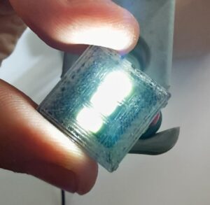
3D object design combining multiple materials within a single volume
The femtosecond laser: a game-changing technology
To make this approach possible, researchers are relying on a tool that is still rarely used in additive manufacturing: the femtosecond laser. A femtosecond is one millionth of a billionth of a second. At this extremely short time scale, the laser delivers considerable power for an infinitesimal instant. This unique characteristic profoundly alters the way matter absorbs energy and makes it possible to melt any material—without having to change the laser’s wavelength (and thus without changing the laser source)—provided that the energy input is ultra-high-frequency (MHz and above).
Thus, unlike continuous-wave lasers used in many industrial processes—whose performance depends on the choice of the laser source’s wavelength relative to the material being processed—the femtosecond laser can process very different materials using the same laser source. Organic or inorganic materials—whether conductors, insulators, or semiconductors—can thus be processed using the same equipment: a single workstation equipped with a print head capable of feeding multiple materials.
At CEMEF, this technology is integrated into an original prototype called FLAM (Filament FemtoLaser Additive Manufacturing). The principle involves feeding the printing zone with filaments heavily loaded with functional particles, while a specially developed optical system focuses the laser beam around the material to precisely control its melting and solidification. This proof of concept, designed in partnership with the French company Cailabs, represents one of today’s major technological challenges: the development of optical systems capable of withstanding the extreme demands of femtosecond laser beams.
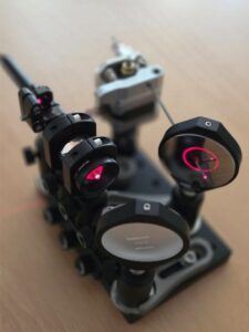
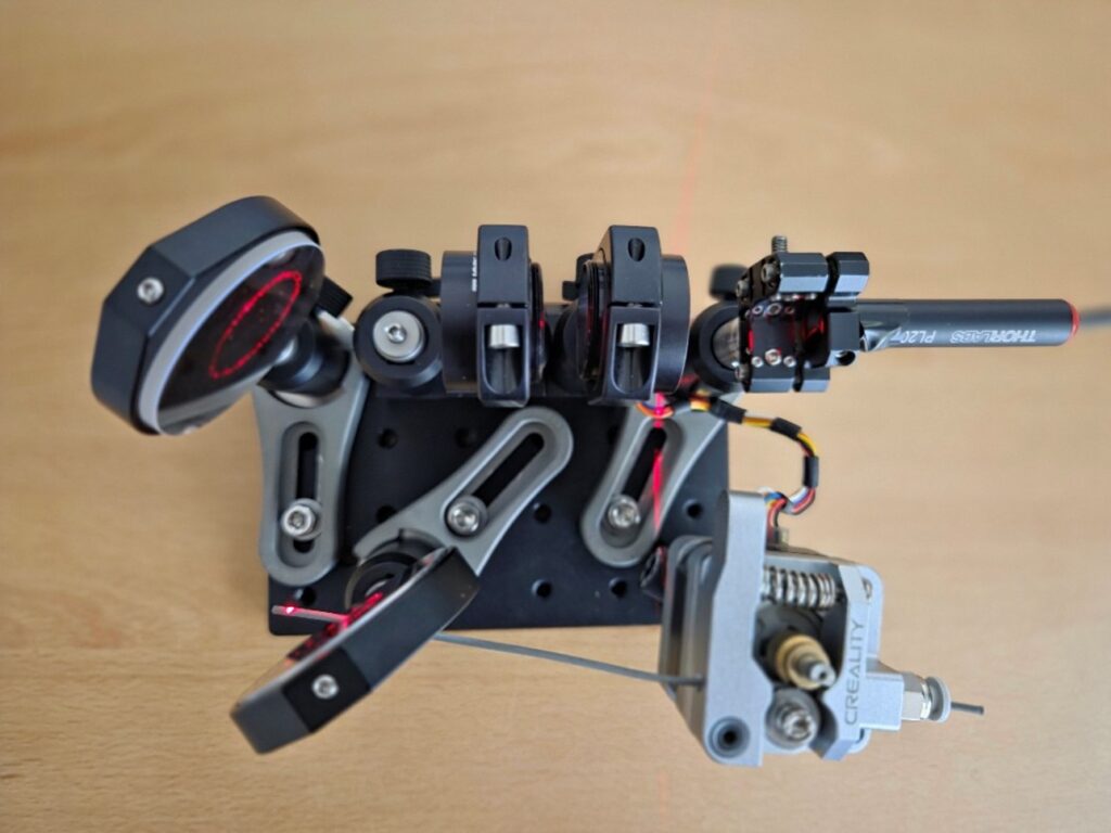
The new print head combines an optical system that projects a converging annular beam with a material feed (Inconel filament shown in the photo), made possible by optics with a central aperture.
From the production line to a single manufacturing station
Beyond the technology itself, this initiative outlines a more comprehensive vision of the industry of the future. Researchers envision a gradual evolution of factories toward manufacturing stations capable of performing, on their own, tasks that currently require a succession of numerous machines and workstations. This approach would make it possible to produce complex objects on a single manufacturing platform, moving directly from the digital model to the final part.
This simplification of processes offers several major advantages. By reducing the number of manufacturing steps, it minimizes intermediate transport, assembly operations, and material waste. It also offers a great deal of design freedom: it becomes possible to directly manufacture complex three-dimensional shapes, repair an existing part locally, or even integrate electronic functions within a mechanical structure itself.
This research illustrates this ambition through numerous potential applications: next-generation printed circuits, metal-ceramic composites, sensors, actuators, smart structures, substrates for power electronics, and even metastructures with unprecedented properties.
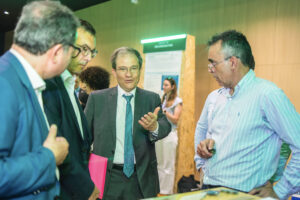
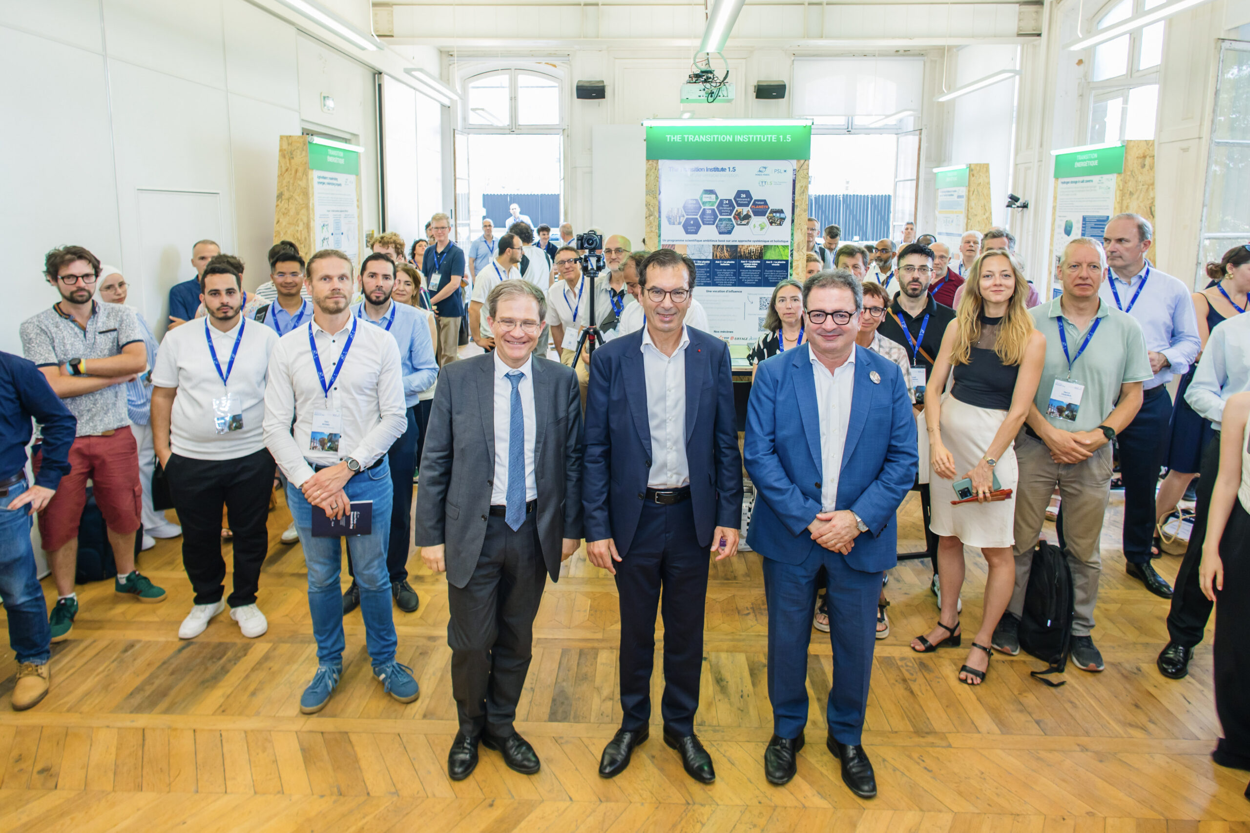
Presentation of the FLAM research initiative at the Mines Paris Research Day 2026. From left to right: El Mouhoub Mouhoud, president of PSL University, Jean-Pierre Farandou, Minister of Labor and Solidarity, Godefroy Beauvallet, director general of Mines Paris – PSL, and Karim Inal, professor at the Center for Materials Forming (CEMEF) at Mines Paris – PSL.
An innovation designed to help decarbonize industry
One of the most remarkable aspects of this initiative is its environmental impact. Additive manufacturing already helps minimize material waste by producing only the necessary amount. The approach taken here goes a step further by seeking to eliminate several particularly resource-intensive processes.
The prototype developed at CEMEF operates without water and produces no waste. It is currently set up on an optical bench, with a fixed print head and a movable sample holder. The miniaturization of the proof-of-concept developed with Cailabs will enable another configuration: a movable print head mounted on a Yaskawa robot at CEMEF, a robot capable of performing complex movements. And once again, a French company, GLOphotonics, will supply the special flexible optical cable connecting the moving head to CEMEF’s ultra-high-repetition-rate femtosecond laser source.
Ultimately, this could also make it possible to directly use certain recycled raw materials—such as metal salts from the WeeeCycling plant in France—to transform them into metal during the laser printing process, thereby opening up new prospects for the circular economy.
The challenges are particularly evident in the field of printed circuit boards, which are ubiquitous in all electronic equipment. Their conventional manufacturing consumes considerable amounts of resources: approximately 1.09 metric tons of water are used to produce a single square meter of printed circuit board, while 740 kg of toxic effluents must be treated. Each square meter also generates nearly 283 kg of CO₂ equivalent, in addition to significant volumes of chemical waste and annual losses of more than 70,000 metric tons of copper in etching baths worldwide.
By eliminating the chemical etching steps in favor of direct additive manufacturing, this approach could help significantly reduce these environmental impacts while strengthening European autonomy in a sector that is now particularly strategic.
Femtolaser-Matter Interaction to Pioneering Tomorrow’s Processes
Behind this technological demonstration lies significant fundamental research. Before considering industrialization, researchers must precisely understand what occurs when the laser’s ultrashort, high-frequency pulses interact with the material during the 3D printing process. Temperature gradients, melt dynamics, solidification, crystal growth, and the development of internal stresses are all phenomena that determine the final properties of the manufactured multi-material structures. This phase is a key step in optimizing print speed and increasing the size of the melt pool.
The development of the FLAM prototype draws on the expertise of several CEMEF teams (multiscale modeling and experimental characterization at the fine scales of matter, filament production, testing, and trials), which are brought together under a cross-disciplinary research initiative within the laboratory. This approach consolidates the deployment of the new process and, ultimately, the production of parts with functional and durable properties perfectly suited to their intended uses.
Collaborative Research in Support of Industrial Transitions
Presented at the Mines Paris Research Day 2026, this initiative fully exemplifies the mission of collaborative research led by Mines Paris – PSL: to transform cutting-edge scientific advances into concrete solutions that address major industrial, environmental, and technological challenges.
To tackle such an ambitious challenge, CEMEF relies on a network of partners that brings together public research institutions, innovative companies, and major industrial groups. Alongside CEMEF, Chimie ParisTech – PSL and the CNRS contribute their scientific expertise, while companies such as Cirly, SynergieCAD, GE HealthCare, L’Oréal Research & Innovation, Safran, Thales, and Naval Group help steer developments toward applications that meet concrete industrial needs. In addition, a collaboration with equipment manufacturers specializing in continuous-wave laser additive manufacturing is underway to explore a new offering: femtosecond technology. This diversity of partners reflects the technology’s cross-cutting potential, with applications spanning electronics, healthcare, transportation, defense, and the manufacturing industries.
Through this initiative, CEMEF offers much more than a new manufacturing technique: it outlines a new way of designing factories, where industrial performance, environmental sustainability, and design freedom now advance hand in hand. This ambition fully embodies the spirit of the Mines Paris Research Day, a true showcase of collaborations that accelerate the transition from research to the innovations of tomorrow.